Surface Mount Solutions (SMS) delivers high-performance PCB assemblies tailored to meet the specific needs of industries worldwide. From tech hubs in Silicon Valley to aerospace sectors in Berlin, our scalable, reliable solutions drive innovation and success in a variety of markets.

SMS provides tailored PCB assemblies to meet the distinct needs of industries across the globe. From aerospace and automotive to tech and telecommunications, our solutions are engineered to address the specific challenges of each region. Explore how SMS delivers scalable, reliable, and high-performance PCBs that drive innovation in your market.
Reliable PCB assemblies for Silicon Valley’s tech and semiconductor companies.

High-performance PCB assemblies for the Bay Area’s leading industries, including tech and aerospace.


Durable, high-reliability PCB assemblies for Phoenix’s aerospace and defense industries.


High-reliability PCB assemblies for Vancouver’s software and telecom applications.


Scalable, high-performance PCBs for tech and manufacturing applications in Mexico City.


Scalable PCB assemblies for AI and tech applications in Toronto’s booming tech industry.

Scalable PCB assemblies for biotech and telecom industries in the Research Triangle.


Reliable, compliant PCBs for Boston’s biotech, medical, and communications applications.

Scalable PCB assemblies for Dublin’s tech and data center sectors, supporting growth and innovation.

High-reliability PCBs for London’s aerospace, telecom, and defense applications.

Scalable PCB assemblies for Stockholm’s startup and telecommunications industries.


High-precision PCB assemblies for Paris’s AI, IoT, and big data industries, supporting innovation.

High-precision, scalable PCB assemblies for Seoul’s electronics and telecommunications industries.


Durable, high-performance PCBs for São Paulo’s automotive and industrial applications.

Scalable, high-performance PCB assemblies for Shenzhen’s hardware and electronics industries.

Scalable, high-reliability PCB assemblies for Hong Kong’s financial and manufacturing industries.

Scalable, energy-efficient PCB assemblies for Sydney’s tech and IoT industries.

High-precision PCB assemblies for Singapore’s finance, tech, and IoT applications.

Cost-effective, scalable PCB assemblies for Bangalore’s tech and electronics sectors.

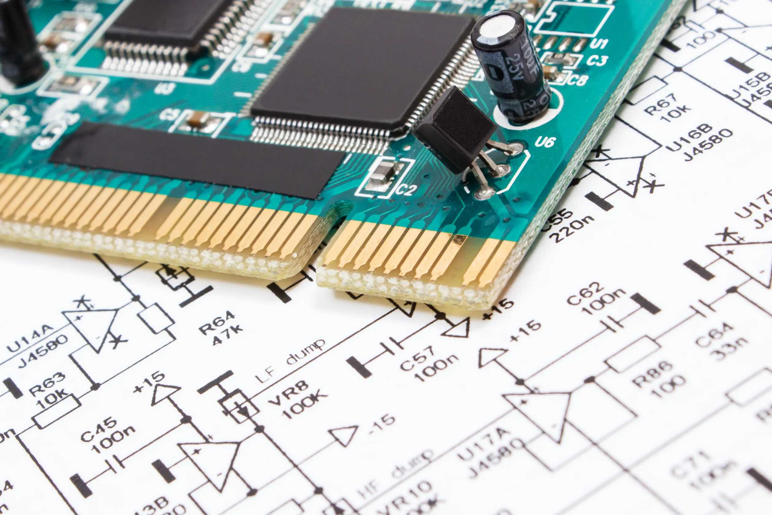
Turning complex circuit board designs into reliable, high-quality products requires an efficient and detail-oriented process. Our step-by-step approach eliminates common manufacturing obstacles, ensuring smooth production, superior quality, and on-time delivery. Each stage is designed to tackle potential pain points, giving you confidence that your PCB assembly project will be handled with precision and expertise.
Every successful project starts with a strong foundation. Our engineers work closely with your team to review your design files, providing Design for Manufacturability (DFM) feedback. This early-stage consultation helps prevent costly revisions and optimizes your design for a seamless transition to production.
Component sourcing can be challenging, especially when balancing cost and lead times. Our experienced procurement team handles all aspects of materials procurement, ensuring that the best-quality components are used and that your project stays on schedule, even for complex printed circuit board designs.
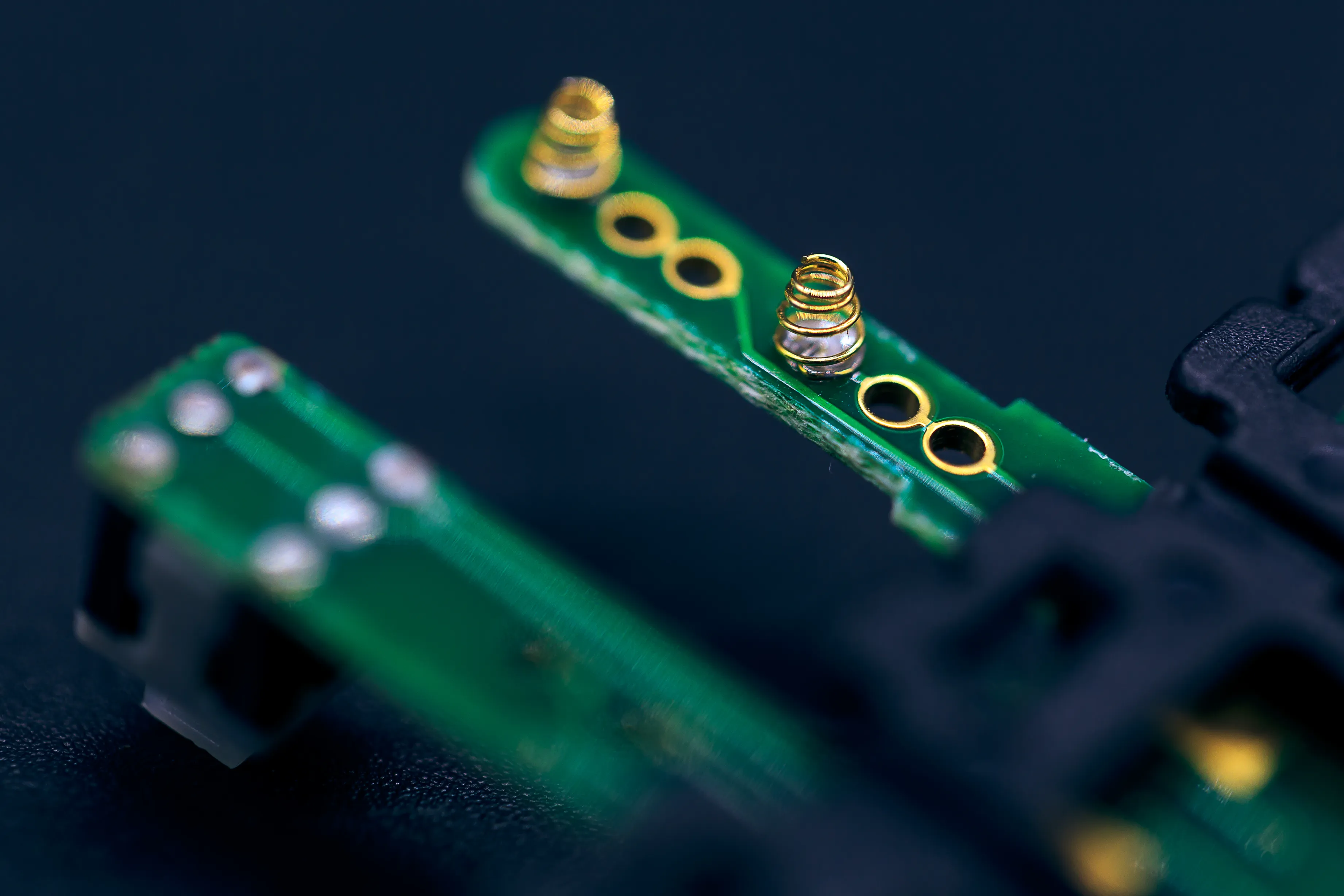
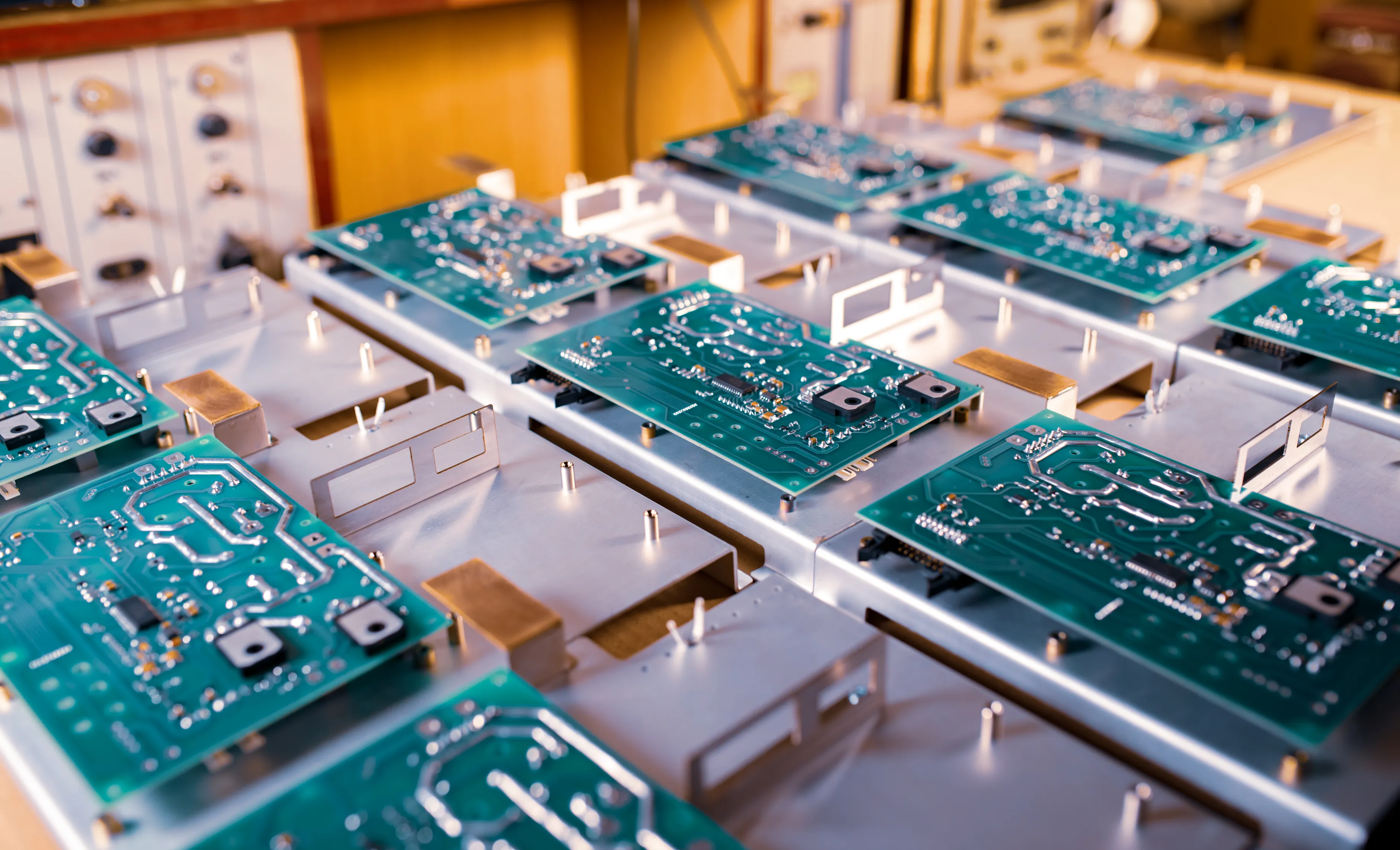
We use state-of-the-art surface mount technology (SMT) and through-hole assembly techniques to build your circuit boards with the highest accuracy and consistency. Our advanced equipment and skilled technicians ensure precise placement of even the smallest components for a robust, reliable build.
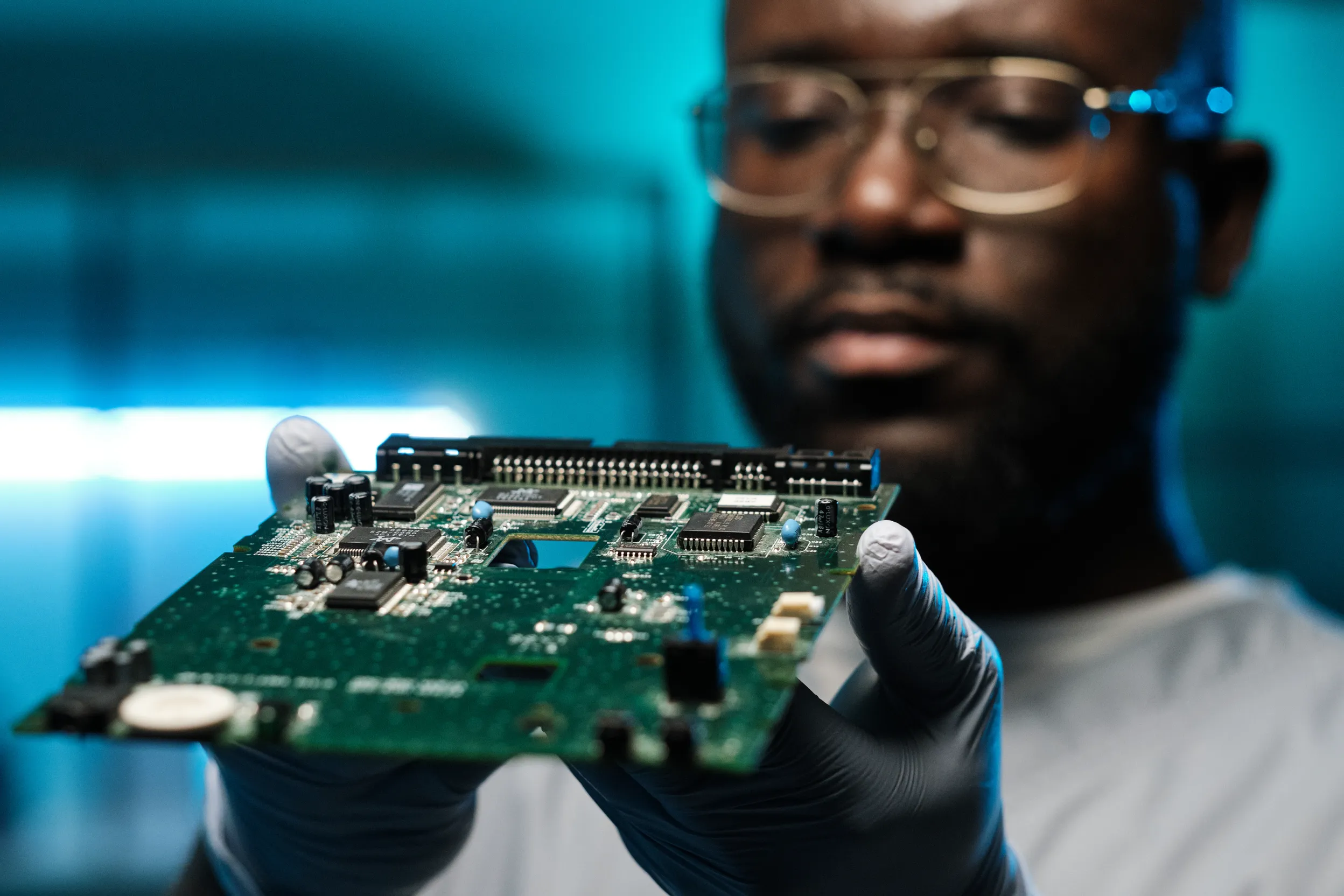
Quality is our top priority. Each assembly goes through multiple inspection stages, including Automated Optical Inspection (AOI), X-ray testing, and comprehensive functional testing. This ensures every circuit board meets stringent standards and performs as expected.
Once testing is complete, your product is prepared for delivery. Whether you need full box builds, special packaging, or local delivery, our logistics team ensures that each project arrives on time and ready for deployment.
Get in touch today to discuss how we can turn your complex designs into reliable, high-quality products.
Our turnkey PCB solutions guarantee precise PCB assembly and on-time delivery. With over 20 years of experience, we offer tailored services to meet your needs, with competitive pricing and quality you can rely on.
Complete Turnkey PCB Solution
20+ Years of Experience
Customer-Centric Communication
Cost-Effective Manufacturing
Scalable Manufacturing
State-of-the-Art Technology
Whether you need a quick-turn solution or end-to-end turnkey services, our capabilities are designed to support every stage of your PCB assembly process.
With advanced technologies, flexible lead times, and a commitment to quality, we tailor our services to your specific project requirements.
Depending on customer requests, projects can be completed in as little as 2-4 days, ideal for urgent needs.
A cost-effective solution with a lead time of 5 days (assembly only).
Comprehensive solutions, including procurement and assembly, completed in 10-15 days, depending on part availability.
Advanced SMT capabilities for high-precision components, handling placements down to 01005 with fine-pitch BGA and QFN.
Precision through-hole technology using selective soldering for mixed-technology assemblies, ensuring robust connections.
Accommodating boards up to 18”x15” with custom panelization options for efficient production and cost savings.
Automated Optical Inspection (AOI) and inline cleaning ensure that each PCB assembly is free from defects and contaminants.
Functional testing, BGA X-ray inspection, and rework solutions like BGA reballing to guarantee flawless performance.
Providing full reels and properly labeled components ensures uninterrupted production. Avoid loose parts and supply at least 5 inches of cut tape for feeder compatibility.
See More Details
See More Details
Full Reels Preferred: Whenever possible, provide full reels to minimize machine downtime and ensure uninterrupted production.
Cut Tape: If cut tape is necessary, it must be at least 5 inches long for proper feeder handling.
Machine Loss: Add 2% for all passive components to account for machine loss, and 4% for 0402 caps and resistors.
Loose Components: Loose parts must be hand-placed, which increases time and cost—please avoid whenever possible.
Labeling: Clearly label reels or trays with the customer part number and a complete component description, including value and part type.
IC Packaging: Integrated Circuits (ICs) should ideally be on tape and reel; however, if tubes are used, ensure all components face the same direction and the tube is properly labeled.
Boards must include fiducials, silkscreen reference markers, and adequate component clearance. Consider panelizing for smaller boards to maximize efficiency.
See More Details
See More Details
Fiducials: Boards and panels must include fiducials for accurate alignment during assembly.
Silkscreen: Ensure reference designators and polarity markers are visible on the silkscreen.
Component Clearance: Components should not be placed within 0.080 inches of the edge of the board to avoid damage.
Panelization: For boards smaller than 3x4 inches, consider panelizing. Ideal panel size is approximately 8x10 inches with a 0.25” border.
Double-Sided Boards: For double-sided assemblies, passive components should be placed on the bottom side when possible.
Submit Gerber files, a current BOM, and CAD data for machine programming. Include an audit sheet for any shortages, and consider providing a sample board.
See More Details
See More Details
Gerber Files: Gerber data is required to produce the stencil and ensure proper layout for panelized boards.
BOM (Bill of Materials): Provide an accurate BOM for the current build, including all parts and values, for assembly accuracy.
CAD Data: CAD data is required for machine programming and ensuring precise component placement.
Audit Sheet: Include an audit sheet listing all shortages and discrepancies in the provided parts to avoid delays in the assembly process.
Sample Board (Optional): Providing a sample board can greatly aid in the accurate assembly of your production run.
To guarantee a smooth and efficient assembly process, it's essential to follow these kitting guidelines. By properly preparing your parts, boards, and data, we can ensure accurate and timely production while minimizing delays and errors.
Contact SMS to take advantage of our turnkey PCB assembly services, ensuring fast lead times, precision, and quality.